MetroCal™
for Stage Mapping
|
- The most widely used application of MetroCal: Artifact for mapping XY stages in metrology tools and electrical test equipment - Targets on MetroCal wafers can be used for both mapping and stage repeatability tests.
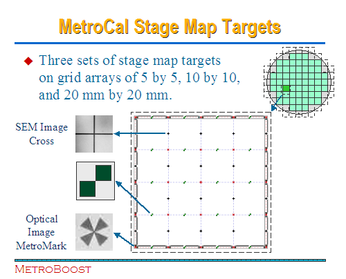
- Three different sets of stage map targets are available on 5 mm by 5 mm grids. The array of crosses can be used for mapping stages of SEM and Focused Ion Beam tools. The other two targets, MetroMarks and double squares, are suitable for use with optical camera images. Those targets are filled with gratings to provide some level of image contrast for practically any illumination condition.
- Targets are printed on the entire wafer surface area up to 1 mm from the wafer edge. Even the partial fields are printed. The benefit is more coverage on the wafer so that you can map the stage close to the wafer's edge.
- For stage mapping application, customers are primarily concerned about pattern placement accuracy of the mapping targets. The capabilities of the advanced scan and repeat exposure tools used in printing MetroCal wafers are relied upon for optimal manufacturing. Production lots are monitored by measuring the stitching overlay targets in all fields and on a few wafers per lot. While stitching overlay is not a measure of pattern placement accuracy, the results provide an upper bound on the variation in placement of any field relative to its four neighbors. Finally, for an absolute pattern placement accuracy verification, one 200 mm wafer was submitted for traceable measurements.
- Stitching overlay targets in all fields are measured on five wafers per lot. The results reveal that the variation in placement of any field relative to its neighbors is 20 nm or less.
- One 200 mm wafer was sent for traceable measurements of absolute pattern placement accuracy using a modified Leica Ipro. Certification measurements were carried out at 20°C which is not the same as the fab operating temperature. After accounting for wafer expansion corresponding to 1.5°C, the remaining results indicate maximum pattern placement error (from an ideal grid) of the order of 100nm in X or Y direction for any of the targets measured on that wafer.
- Stage movement error can be mapped by using any of the three sets of mapping features spaced every 5 or 10 or 20 mm. A two-dimensional error vector map can be generated by driving the stage to mapping target locations and comparing actual stage landing positions to the ideal target locations. (Here, we ignore the pattern placement error for all MetroCal mapping targets.) The resulting error vector map can then be used to compensate for the motion of the X-Y stage over the entire 300mm wafer diameter. Using MetroCal wafers as stage mapping artifacts and assuming zero pattern placement error for MetroCal mapping targets, stage movement accuracy of 1 micron (mean plus three sigma error in X or Y) has been achieved on metrology tool stages.
- MetroCal wafer is compatible with heating and cooling cycles that product wafers may be subjected to as part of electrical tests. Because it has the same coefficient of thermal expansion as the product wafers, MetroCal can be used to carry out stage mapping and/or positioning tests at the extremes of the operating temperature range for the test equipment.
- Even when another substrate is used for mapping the stage, MetroCal can be used to test stage positioning accuracy on a 5 mm by 5 mm grid. This makes MetroCal especially useful for pre-purchase equipment evaluations and tool demonstrations.
|
>> Back to MetroCal Description
Home | Products | Downloads | Contact Us
|